Compound semiconductors significantly enhance electronic devices, enabling them to be smaller, faster, and more energy-efficient.
They significantly increase the energy we can harness from solar panels and empower our electric cars to travel much farther. These innovations are crucial for improving the environment and are essential for achieving Net Zero emissions. Furthermore, they guarantee that our tablets and smartphones can send and receive data at lightning-fast speeds.
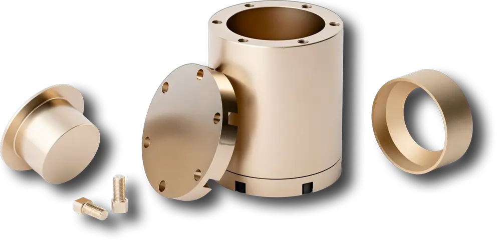
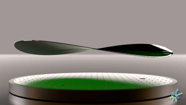
Ingot
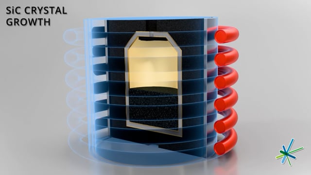
Crystal Growth (SiC)
Physical Vapor Transport (PVT) is a popular method for growing single crystals of compound semiconductors, such as silicon carbide (SiC). It is highly regarded for its capability to produce high-purity and defect-free crystals. The primary development focus is improving crystal quality, increasing ingot size, and reducing production costs.
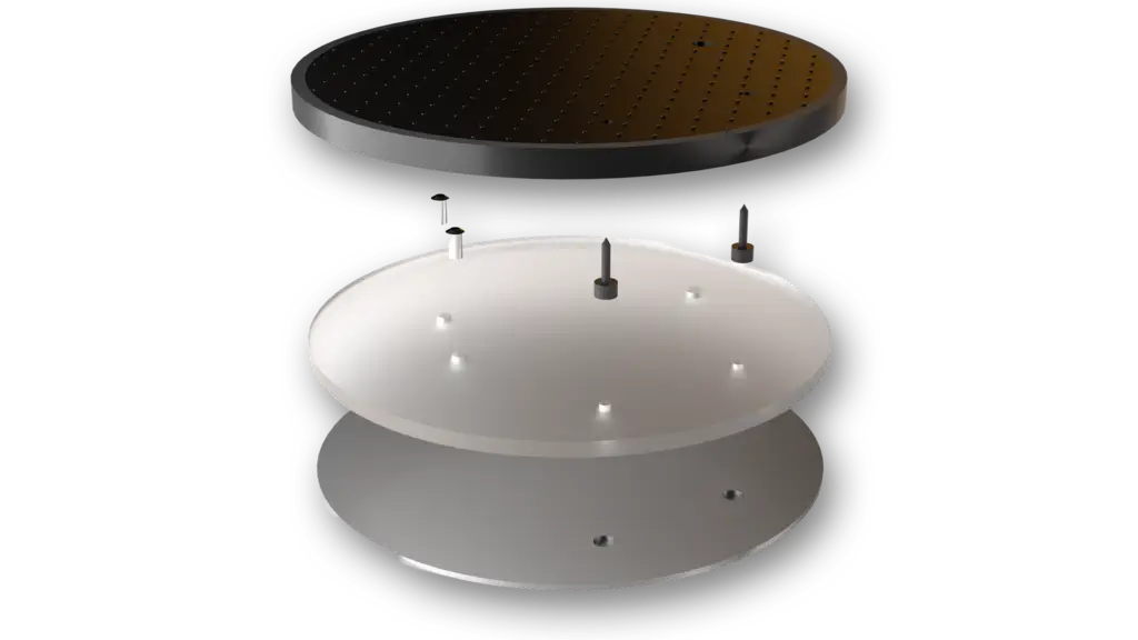
With its high-temperature stability, high purity, and high chemical resistance, Tantalum Carbide (TaC) coatings in PVT furnaces suppress contamination in contact with graphite, extend graphite component life, and maintain sublimation stoichiometry.
In-depth technical information and details for TaC coatings
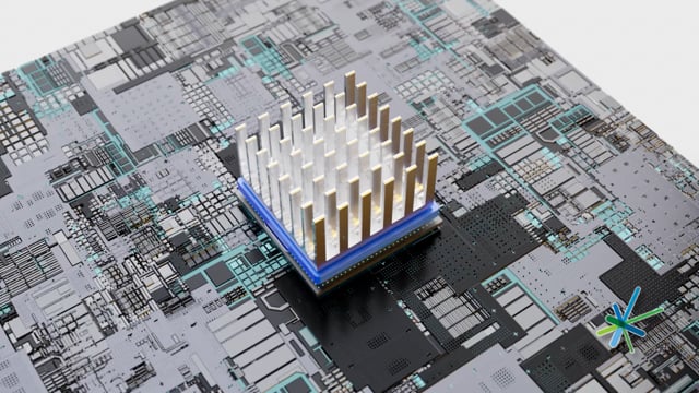
Compound semiconductor epitaxy involves depositing thin films of compound semiconductor materials onto crystalline substrates to create artificial crystal structures. This technology is essential for harnessing the electrical properties of compound semiconductors in advanced devices. The entire setup must be constructed with high-purity materials that withstand high temperatures and harsh chemical environments.
Tantalum carbide (TaC) is used as a protective coating for graphite components in compound semiconductor epitaxy. It provides thermal stability and chemical resistance against corrosive gases and high temperatures, ensuring the durability of graphite parts used to grow materials like silicon carbide (SiC) and gallium nitride (GaN).
In-depth technical information and details for TaC coatings
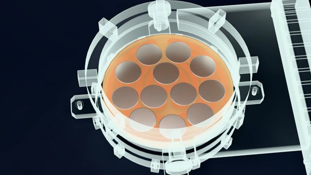
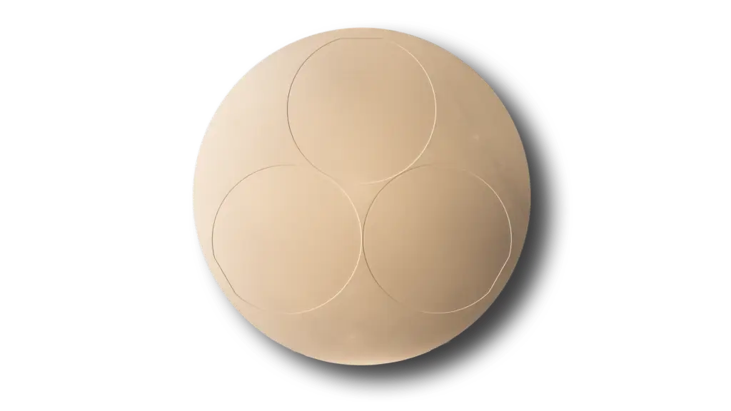
Compound semiconductor ion implantation is a process in which ions are accelerated and implanted into a semiconductor material made up of multiple elements, such as Silicon Carbide (SiC), Gallium Arsenide (GaAs), Indium Phosphide (InP), or Gallium Nitride (GaN). This technique allows for precise control over the electrical properties of the material by introducing specific dopants at designated depths within the semiconductor lattice. As a result, it enables the creation of tailored electronic devices with desired functionalities.
High-temperature ion implantation followed by annealing is standard in SiC device fabrication. Ion implantation at elevated temperatures increases the dynamic annealing and helps to eliminate point defects.
An “Electrostatic Chuck” is a specialized chuck used in ion implantation machines to hold and accurately position compound semiconductor wafers during the ion implantation process.
Dielectrics, pyrolytic Boron Nitride (pBN), with its unique high-temperature resistivity profiles, enabled the high-temperature chucking operation beyond the conventional ceramic Electrostatic Chucks (ESC) capability. Combining both Pyrolytic graphite coating and graphite, the dual-functioned pBN ESC achieved high chuck force and good thermal uniformity with a fast response at elevated temperatures. This ESC technology provides a viable solution to the wafer heating and handling challenges in the SiC and GaN ion implantation application
In-depth technical information and details for pBN Heaters and Electrostatic Chucks
Heat is one of the major threats to today’s electronic components and assemblies. It can shorten their service life and compromise reliability. As designers and manufacturers strive to create smaller, faster assemblies, the need for effective heat dissipation becomes increasingly important.
Hexagonal Boron Nitride (BN) and Spherical Alumina (SA) fillers address this issue. When added to polymers, BN and SA enhance heat dissipation, which helps improve the longevity and reliability of electronic components. Compared to fused silica, aluminum oxide, and aluminum nitride, BN and SA excel in thermal conductivity, with some composites achieving levels as high as 15 W/mK.
In-depth technical information and details for Boron Nitride and Spherical Alumina.
Compound semiconductors are advanced materials with distinct properties that set them apart from traditional semiconductors. These versatile materials play a crucial role in a wide range of applications, from…
from powering electric vehicles and
converting sunlight into energy in solar panels to
enabling communication in satellites and spacecraft.
Additionally, they are essential components in smartphones, enhancing performance and efficiency. As technology continues to evolve, future innovations such as autonomous vehicles and sophisticated artificial intelligence systems will increasingly rely on the unique capabilities of compound semiconductors, highlighting their importance in shaping the future of technology.
Products Used in Compound Semiconductor Processes
Ceramics
Have questions or need more information about how we assist customers in thinking big with their semiconductor innovations?